
| Admissions | Accreditation | Booksellers | Catalog | Colleges | Contact Us | Continents/States/Districts | Contracts | Examinations | Forms | Grants | Hostels | Honorary Doctorate degree | Instructors | Lecture | Librarians | Membership | Professional Examinations | Programs | Recommendations | Research Grants | Researchers | Students login | Schools | Search | Seminar | Study Center/Centre | Thesis | Universities | Work counseling |
|
Electron Microscopy What are Electron Microscopes? Where did Electron Microscopes Come From? How do Electron Microscopes Work? What is the SEM? How does the SEM work? What are Electron Microscopes? Electron Microscopes are scientific instruments that use a beam of highly energetic electrons to examine objects on a very fine scale. This examination can yield the following information: Topography The surface features of an object or "how it looks", its texture; direct relation between these features and materials properties (hardness, reflectivity...etc.) Morphology The shape and size of the particles making up the object; direct relation between these structures and materials properties (ductility, strength, reactivity...etc.) Composition The elements and compounds that the object is composed of and the relative amounts of them; direct relationship between composition and materials properties (melting point, reactivity, hardness...etc.) Crystallographic Information How the atoms are arranged in the object; direct relation between these arrangements and materials properties (conductivity, electrical properties, strength...etc.) Where did Electron Microscopes Come From? Electron Microscopes were developed due to the limitations of Light Microscopes which are limited by the physics of light to 500x or 1000x magnification and a resolution of 0.2 micrometers. In the early 1930's this theoretical limit had been reached and there was a scientific desire to see the fine details of the interior structures of organic cells (nucleus, mitochondria...etc.). This required 10,000x plus magnification which was just not possible using Light Microscopes. The Transmission Electron Microscope (TEM) was the first type of Electron Microscope to be developed and is patterned exactly on the Light Transmission Microscope except that a focused beam of electrons is used instead of light to "see through" the specimen. It was developed by Max Knoll and Ernst Ruska in Germany in 1931. The first Scanning Electron Microscope (SEM) debuted in 1942 with the first commercial instruments around 1965. Its late development was due to the electronics involved in "scanning" the beam of electrons across the sample. An excellent article was just published in Scanning detailing the history of SEMs and I would encourage those interested to read it. How do Electron Microscopes Work? Electron Microscopes(EMs) function exactly as their optical counterparts except that they use a focused beam of electrons instead of light to "image" the specimen and gain information as to its structure and composition. The basic steps involved in all EMs: 1. A stream of electrons is formed (by the Electron Source) and accelerated toward the specimen using a positive electrical potential 2. This stream is confined and focused using metal apertures and magnetic lenses into a thin, focused, monochromatic beam. 3. This beam is focused onto the sample using a magnetic lens 4. Interactions occur inside the irradiated sample, affecting the electron beam These interactions and effects are detected and transformed into an image The above steps are carried out in all EMs regardless of type. A more specific treatment of the workings of two different types of EMs are described in more detail: Transmission Electron Microscope Scanning Electron Microscope Types of Electron Microscopes All electron microscopes use electromagnetic and/or electrostatic lenses to control the path of electrons. Glass lenses, used in light microscopes, have no effect on the electron beam. The basic design of an electromagnetic lens is a solenoid (a coil of wire around the outside of a tube) through which one can pass a current, thereby inducing an electromagnetic field. The electron beam passes through the centre of such solenoids on its way down the column of the electron microscope towards the sample. Electrons are very sensitive to magnetic fields and can therefore be controlled by changing the current through the lenses. The faster the electrons travel, the shorter their wavelength. The resolving power of a microscope is directly related to the wavelength of the irradiation used to form an image. Reducing wavelength increases resolution. Therefore, the resolution of the microscope is increased if the accelerating voltage of the electron beam is increased. The accelerating voltage of the beam is quoted in kilovolts (kV). It is now possible to purchase a 1,000kV electron microscope, though this is not commonly found. Although modern electron microscopes can magnify objects up to about two million times, they are still based upon Ruska's prototype and the correlation between wavelength and resolution. The electron microscope is an integral part of many laboratories such as The John Innes Centre. Researchers can use it to examine biological materials (such as microorganisms and cells), a variety of large molecules, medical biopsy samples, metals and crystalline structures, and the characteristics of various surfaces. Nowadays, electron microscopes have many other uses outside research. They can be used as part of a production line, such as in the fabrication of silicon chips, or within forensics laboratories for looking at samples such as gunshot residues. In the arena of fault diagnosis and quality control, they can be used to look for stress lines in engine parts or simply to check the ratio of air to solids in ice cream! Transmission Electron Microscope (TEM) The original form of electron microscopy, Transmission electron microscopy (TEM) involves a high voltage electron beam emitted by a cathode and formed by magnetic lenses. The electron beam that has been partially transmitted through the very thin (and so semitransparent for electrons) specimen carries information about the structure of the specimen. The spatial variation in this information (the "image") is then magnified by a series of magnetic lenses until it is recorded by hitting a fluorescent screen, photographic plate, or light sensitive sensor such as a CCD (charge-coupled device) camera. The image detected by the CCD may be displayed in real time on a monitor or computer. Transmission electron microscopes produce two-dimensional, black and white images. Resolution of the TEM is also limited by spherical and chromatic aberration, but a new generation of aberration correctors has been able to overcome or limit these aberrations. Software correction of spherical aberration has allowed the production of images with sufficient resolution to show carbon atoms in diamond separated by only 0.089 nm and atoms in silicon at 0.078 nm at magnifications of 50 million times. The ability to determine the positions of atoms within materials has made the TEM an indispensable tool for nano-technologies research and development in many fields, including heterogeneous catalysis and the development of semiconductor devices for electronics and photonics. In the life sciences, it is still mainly the specimen preparation which limits the resolution of what we can see in the electron microscope, rather than the microscope itself. At JIC we have a high voltage (200kV) TEM, which was installed in 2008. We have two digital cameras on it, one is higher resolution than the other, so that the need for developing and printing film has been negated. Our TEM is designed for use with biological samples and is capable of resolving to better than 1nm. It is also capable of 3-D tomography which involves taking a succession of images whilst tilting the specimens through increasing angles, which can then be combined to form a three-dimensional image of the specimen. Scanning Electron Microscope (SEM) Unlike the TEM, where the electrons in the primary beam are transmitted through the sample, the Scanning Electron Microscope (SEM) produces images by detecting secondary electrons which are emitted from the surface due to excitation by the primary electron beam. In the SEM, the electron beam is scanned across the surface of the sample in a raster pattern, with detectors building up an image by mapping the detected signals with beam position. SEM image of a fly's foot plate showing the drawing of a fly's foot SEM image of a fly's foot taken at JIC in 2006 From "Micrographia", by Robert Hooke, 1665: plate showing the drawing of a fly's foot TEM resolution is about an order of magnitude better than the SEM resolution. Our TEM can easily resolve details of 0.2nm. Our two SEMs at JIC are both relatively recent acquisitions and are high-resolution instruments capable of about 2 nm resolution on biological samples. Because the SEM image relies on electron interactions at the surface rather than transmission it is able to image bulk samples and has a much greater depth of view, and so can produce images that are a good representation of the 3D structure of the sample. SEM images are therefore considered to provide us with 3D, topographical information about the sample surface but will still always be only in black and white. In the SEM, we use much lower accelerating voltages to prevent beam penetration into the sample since what we require is generation of the secondary electrons from the true surface structure of a sample. Therefore, it is common to use low KV, in the range 1-5kV for biological samples, even though our SEMs are capable of up to 30 kV. At JIC we currently have two SEMs, both with high-resolution capabilities, digital imaging facilities and cryo-systems which enable them to be used for looking at frozen-hydrated specimens. Sample Preparation Materials to be viewed in an electron microscope generally require processing to produce a suitable sample. This is mainly because the whole of the inside of an electron microscope is under high vacuum in order to enable the electron beam to travel in straight lines. The technique required varies depending on the specimen, the analysis required and the type of microscope: Cryofixation - freezing a specimen rapidly, typically to liquid nitrogen temperatures or below, that the water forms ice. This preserves the specimen in a snapshot of its solution state with the minimal of artefacts. An entire field called cryo-electron microscopy has branched from this technique. With the development of cryo-electron microscopy, it is now possible to observe virtually any biological specimen close to its native state. Fixation - a general term used to describe the process of preserving a sample at a moment in time and to prevent further deterioration so that it appears as close as possible to what it would be like in the living state, although it is now dead. In chemical fixation for electron microscopy, glutaraldehyde is often used to crosslink protein molecules and osmium tetroxide to preserve lipids. Dehydration - removing water from the samples. The water is generally replaced with organic solvents such as ethanol or acetone as a stepping stone towards total drying for SEM specimens or infiltration with resin and subsequent embedding for TEM specimens. Embedding - infiltration of the tissue with wax (for light microscopy) or a resin (for electron microscopy) such as araldite or LR White, which can then be polymerised into a hardened block for subsequent sectioning. Sectioning - the production of thin slices of the specimen. For light microscopy, the sections can be a few micrometres thick but for electron microscopy they must be very thin so that they are semitransparent to electrons, typically around 90nm. These ultra-thin sections for electron microscopy are cut on an ultramicrotome with a glass or diamond knife. Glass knives can easily be made in the laboratory and are much cheaper than diamond, but they blunt very quickly and therefore need replacing frequently. Staining - uses heavy metals such as lead and uranium to scatter imaging electrons and thus give contrast between different structures, since many (especially biological) materials are nearly "transparent" to the electron beam. By staining the samples with heavy metals, we add electron density to it which results in there being more interactions between the electrons in the primary beam and those of the sample, which in turn provides us with contrast in the resultant image. In biology, specimens can be stained "en bloc" before embedding and/or later, directly after sectioning, by brief exposure of the sections to solutions of the heavy metal stains. Freeze-fracture and freeze-etch - a preparation method particularly useful for examining lipid membranes and their incorporated proteins in "face on" view. The fresh tissue or cell suspension is frozen rapidly (cryofixed), then fractured by simply breaking or by using a microtome while maintained at liquid nitrogen temperature. The cold, fractured surface is generally "etched" by increasing the temperature to about -95°C for a few minutes to let some surface ice sublime to reveal microscopic details. For the SEM, the sample is now ready for imaging. For the TEM, it can then be rotary-shadowed with evaporated platinum at low angle (typically about 6°) in a high vacuum evaporator. A second coat of carbon, evaporated perpendicular to the average surface plane is generally performed to improve stability of the replica coating. The specimen is returned to room temperature and pressure, and then the extremely fragile "shadowed" metal replica of the fracture surface is released from the underlying biological material by careful chemical digestion with acids, hypochlorite solution or SDS detergent. The floating replica is thoroughly washed from residual chemicals, carefully picked up on an EM grid, dried then viewed in the TEM. Sputter Coating - an ultra-thin coating of electrically-conducting material, deposited by low vacuum coating of the sample. This is done to prevent charging of the specimen which would occur because of the accumulation of static electric fields due to the electron irradiation required during imaging. It also increases the amount of secondary electrons that can be detected from the surface of the sample in the SEM and therefore increases the signal to noise ratio. Such coatings include gold, gold/palladium, platinum, chromium etc. Disadvantages of Electron Microscopy Electron microscopes are very expensive to buy and maintain. They are dynamic rather than static in their operation: requiring extremely stable high voltage supplies, extremely stable currents to each electromagnetic coil/lens, continuously-pumped high/ultra-high vacuum systems and a cooling water supply circulation through the lenses and pumps. As they are very sensitive to vibration and external magnetic fields, microscopes aimed at achieving high resolutions must be housed in buildings with special services. A significant amount of training is required in order to operate an electron microscope successfully and electron microscopy is considered a specialised skill. The samples have to be viewed in a vacuum, as the molecules that make up air would scatter the electrons. This means that the samples need to be specially prepared by sometimes lengthy and difficult techniques to withstand the environment inside an electron microscope. Recent advances have allowed some hydrated samples to be imaged using an environmental scanning electron microscope, but the applications for this type of imaging are still limited. Artefacts It must be emphasised from the outset that every electron micrograph is, in a sense, an artefact. Changes in the ultra-structure are inevitable during all the steps of processing that samples must undergo: material is extracted, dimensions are changed and molecular rearrangement occurs. The best thing we can do is to keep these changes to a minimum by understanding the processes involved so that we make informed choices of the best preparative procedures to use for each sample. Artefacts present themselves in many ways: there could be loss of continuity in the membranes, distortion or disorganisation of organelles, empty spaces in the cytoplasm of cells or sharp bends or curves in filamentous structures that are usually straight, such as microtubules and so on. With experience, microscopists learn to recognise the difference between an artefact of preparation and true structure, mainly by looking at the same or similar specimens prepared in the same or a different way. Scanning electron microscope Block diagram of a typical SEM (Redrawn from J. W. S. HEARLE, J. T. SPARROW, P. M. CROSS, 1972) 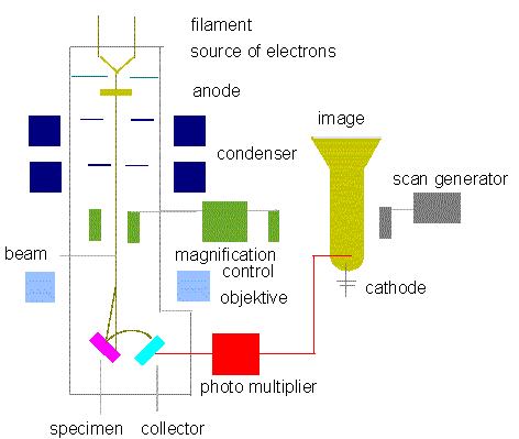 Scanning electron microscopes usually image conductive or semi-conductive materials best. Non-conductive materials can be imaged, either by an environmental scanning electron microscope or more usually by coating the sample with a conductive layer of metal. A common preparation technique is to coat the sample with a layer of conductive material, a few nanometers thick, such as 10nm of gold, from a sputtering machine. This process does, however, have the potential to disturb delicate samples and cover some detail. When using chemical fixation and dehydration as part of the sample preparation, there is often much shrinkage and collapse of delicate structures and so, especially for our interests at JIC in botanical specimens which are highly hydrated, we tend to use the cryo-fixation technique which is far less prone to artefacts. For the TEM, samples are generally prepared by exposure to many nasty chemicals, in order to give good ultra-structural detail which may result in artefacts purely as a result of preparation. This gives the problem of distinguishing artefacts from genuine structures within the specimen, particularly in biological samples. Scientists maintain that the results from various preparation techniques have been compared, and as there is no reason that they should all produce similar artefacts, it is therefore reasonable to believe that electron microscopy features correlate with living cells. In addition, higher resolution work has been directly compared to results from X-ray crystallography, providing independent confirmation of the validity of this technique. Recent work performed on unfixed, vitrified (rapidly frozen, without the use of any chemicals, to form ice without any crystallisation) specimens has also been performed, further confirming the validity of this technique. However, even cryo-fixation techniques are not without their own artefacts of preparation and ice crystal damage, due to the fact that as water freezes it expands, is a common problem when trying to image a large specimen (greater than 200 µm) which cannot be frozen rapidly enough to vitrify the water http://www.unl.edu/CMRAcfem/em.htm http://emf.bsd.uchicago.edu/ http://www.jic.ac.uk/microscopy/intro_em.html http://mse.iastate.edu/microscopy/home.html |