|
Have you ever wondered how chips such as microprocessors, video processors, memories, chipsets etc are created and manufactured? Raw Wafer Fabrication Process The wafer is the substrate where the chips will be built on. Raw wafers are made of silicon, which comes from beach sand. They are created through a method called Czochralski process, where a seed crystal (a piece of silicon crystal) is mounted on a rod and then dipped into molten silicon. The rod is pulled upwards and rotated at the same time, making a big cylindrical piece of silicon crystal, also known as ingot. The ingot resulted from this process measures from three to six feet (one to two meters) long and can have up to 12 inches (300 mm) in diameter (this is where terms like 12-inch or 300-mm wafers come from). The ingot is then sliced into wafers. These wafers are polished and sent to the chip manufacturers. As mentioned, these raw (”virgin“) wafers are where the chips will be manufactured on. 
Photolithography Chips are mounted on the wafer through a process called photolithography. Under this process, chemicals sensitive to ultraviolet light are used. When exposed to ultraviolet light, they can become ”soft“ or ”hard“. So basically this process consists in blocking the ultraviolet light from the chemicals applied to the wafer using stencils (the masks created by the engineers), removing the ”soft“ parts, and then repeating the process again with another mask, until the chip is finished. 
Of course each mask has a different pattern and they tell how the transistors and wires inside the chip will be manufactured. The numbers of masks used vary depending on the project. A Pentium 4 processor, for example, uses 26 masks. Let’s see exactly how this process is done. Photolitography (Cont’d) The first thing that is done to the raw wafer is to grow silicon dioxide (SiO2) on it, by exposing the wafer to extreme heat and gas. This growth is similar to the way rust grows on metal when exposed to water, but it happens faster. Next the wafer is coated with a substance called photoresist, which becomes soluble when exposed to ultraviolet light. The first mask is applied and the wafer is exposed to ultraviolet light. The ”soft“ part of photoresist is removed using solvent and then the parts of the silicon dioxide layer that were revealed are removed in a process called etching. The rest of the photoresist is removed, so now we have the wafer with a silicon dioxide layer with the same shape as the first mask. Another silicon dioxide layer is applied on the wafer, a polysilicon layer is applied on top of it and then another photoresist layer is applied on top of them. The second mask is applied and the wafer is exposed to ultraviolet light again. The ”soft“ part of photoresist is removed using solvent and then the parts of the polysilicon and silicon dioxide layers that were revealed are etched away. The rest of the photoresist is removed, so now we have the wafer with a silicon dioxide layer with the same shape as the first mask and on top of it a polysilicon and silicon dioxide layers with the same shape as the second mask. After these two steps, a process called doping (or ionization) takes place. Here the exposed areas of the wafer are bombed with various ions, to alter the way the exposed areas conduct electricity. The exposed areas will be transformed either into a P-type semiconductor (i.e., positively charged) or into a N-type semiconductor (i.e., negatively charged), depending on the chemicals used: phosphorus, antimony and arsenic are typically used to create a N-type semiconductor layer, while boron, indium and gallium are typically used to create a P-type semiconductor layer. The stacking of semiconductor layers will create the transistors. The layering and masking are repeated, following the layout of the next mask. A metal is then dropped on the wafer, filling eventual holes that were created to make electrical connections between the layers. Another masking and etching processes are done to add the electrical connections. This process is repeated all over again until the chip is done, i.e., all masks were used. The exact manufacturing process and number of layers depends on the component being manufactured. For a Pentium 4 processor, it uses 26 masks and 7 metal layers. 
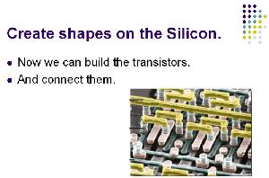
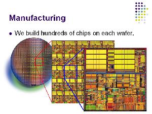
Figure 3: Transistors built inside the chip and the metal connection between them. Figure 4: Wafer with Pentium 4 processor chips after being manufactured. The chips on the wafer are then tested and the wafer is sent to the next step on the chip manufacturing process, where the chips are cut from the wafer, have their terminals attached and are packed. After that they are tested, labeled and sold. 
Clean Room All the processes described take place inside a clean room. You may have already seen some pictures of people working inside a clean room with special clothes, called ”bunny suits“. 
Figure 5: Bunny suits. Since we are talking about microscopic transistors, even the smallest particle of dust can contaminate and destroy the chip, see some examples in Figure 6. 
Figure 6: Even the smallest dust particle can destroy the chip. http://www.hardwaresecrets.com/printpage/How-Chips-are-Manufactured/252 |
